Engineering the Smallest Crack in the World
Graphene-based technique creates the smallest gaps in nanostructures
Published Date
Article Content

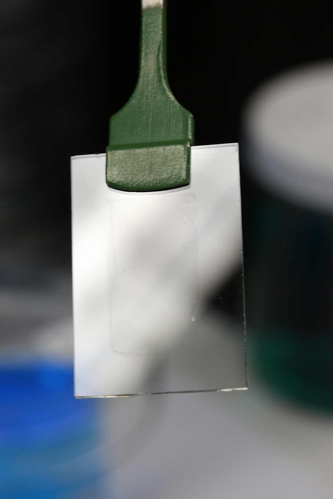
A single layer of graphene shown on a slide.
A new procedure will enable researchers to fabricate smaller, faster, and more powerful nanoscale devices ─ and do so with molecular control and precision. Using a single layer of carbon atoms, or graphene, nanoengineers at the University of California, San Diego have invented a new way of fabricating nanostructures that contain well-defined, atomic-sized gaps. The results from the UC San Diego Jacobs School of Engineering were published in the January issue of the journal Nano Letters.
Structures with these well-defined, atomic-sized gaps could be used to detect single molecules associated with certain diseases and might one day lead to microprocessors that are 100 times smaller than the ones in today’s computers.
The ability to generate extremely small gaps ─ known as nanogaps ─ is highly desirable in fabricating nanoscale structures, which are typically used as components in optic and electronic devices. By decreasing the spacing between electronic circuits on a microchip, for example, one can fit more circuits on the same chip to produce a device with greater computing power.
A team of Ph.D. students and undergraduate researchers led by UC San Diego nanoengineering professor Darren Lipomi demonstrated that the key to generating a smaller nanogap between two nanostructures involves using a graphene spacer, which can be etched away to create the gap.
Graphene is the thinnest material known: it is simply a single layer of carbon atoms and measures approximately 0.3 nanometers (nm), which is about 100,000 times thinner than a human hair. The technique developed by Lipomi’s team overcomes some of the limitations of standard fabrication methods, such as photolithography and electron-beam lithography. By comparison, the smallest nanogaps that can be generated using the standard methods are 10‒20 nm wide.
“Making a nanogap is interesting from a philosophical standpoint,” said Lipomi. “While most efforts in nanotechnology focus on making materials, we’ve essentially made nothing ─ but with controlled dimensions.”
Making “nothing”
The method for making nanogaps begins with the production of thin films in which a single layer of graphene is sandwiched between two gold metal sheets. First, graphene is grown on a copper substrate, and then layered on top with a sheet of gold metal. Because graphene sticks better to gold than to copper, the entire graphene single-layer can be easily removed and remains intact over large areas. Compared to other techniques that are used to produce similar layered structures, this method allows graphene to be transferred to gold film with minimal defects or contamination.
“This new method, which we developed in our lab, is called metal-assisted exfoliation. This is the only way so far in which we can place single-layer graphene between two metals and ensure that it contains no rips, cracks, folds, or unwanted chemical species,” said Alex Zaretski, a graduate student in Lipomi’s research group who pioneered the technique and is the first author of the study. “Metal-assisted exfoliation can potentially be useful for industries that use large areas of graphene.”

Alex Zaretski, a graduate student in the NanoEngineering Department at UC San Diego Jacobs School of Engineering and lead author of the paper.
Once the gold/graphene composite is separated from the copper substrate, the newly exposed side of the graphene layer is sandwiched with another gold sheet to produce the gold:single-layer graphene:gold thin film.
The films are then sliced into 150 nm-wide nanostructures. Finally, the structures are treated with oxygen plasma to remove graphene. Scanning electron micrographs of the structures reveal extremely small nanogaps between the gold layers.
Nanogap applications
One potential application for this technology is in ultra-sensitive detection of single molecules, particularly those that are characteristic of certain diseases. When light is shined upon structures with extremely small gaps, the electromagnetic field that is confined within the gap becomes enormously enhanced. This enhanced electromagnetic field, in turn, increases the signal produced by any molecule within the gap.
“If some disease marker comes in and bridges the gap between the nanostructures, you would observe a change in the light scattering from the nanogap that would correspond to whether the disease was present or not,” said Lipomi.
While the technique reported in this study can produce nanostructures suitable for optical applications, it exhibits a major drawback for electronic applications. Raman spectroscopic measurements of the gold nanostructures reveal that small amounts of graphene still remain between the gold layers after being treated with oxygen plasma. This means that only the graphene exposed near the surfaces of the gold nanostructures can be removed so far. Having graphene still in the structures is not desirable for electronic devices, which require an entire gap between the structures. The team is working to figure out how to solve this problem.

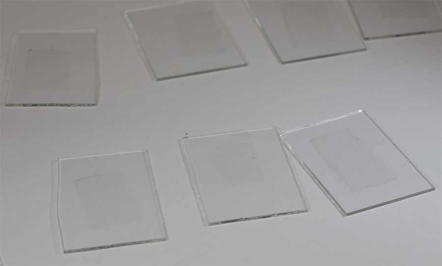
Slides containing single-layer graphene samples.
In the future, the team would also like to explore ways to vary the thickness of the well-defined gap between the structures by increasing the number of graphene layers.
“For optical applications, it would be desirable to have gaps that are a little bit bigger than what we’ve generated. We just wanted to show, in principle, the smallest gap size that is possible to achieve,” said Lipomi.
This work was supported by the laboratory startup funds from UC San Diego. A.Z. acknowledges fellowships from SoCal Clean Energy Technology Acceleration Program from the von Liebig Center at UC San Diego sponsored by the US Department of Energy, and from the National Science Foundation Graduate Research Fellowship Program, DGE-1144086. H.M. acknowledges support from the Calit2-Qualcomm Institute Summer Undergraduate Research Scholars program. B.M., T.D., and A.R.T. acknowledge support from the Office of Naval Research (Award No. N000141210574) and a DURIP grant (Award No. N000141310655). This work was performed in part with the support of the Calit2 Nano3 facilities and staff at UC San Diego.
Share This:
Stay in the Know
Keep up with all the latest from UC San Diego. Subscribe to the newsletter today.


