Moving Data with the Speed of Light: Polaris Electro-Optics Rides the Wave of the Future


Published Date
Article Content
From YouTube to AI, our use of digital information technology has exploded, and, with it, the need to seamlessly move data from one location to another.
Cory Pecinovsky, founder and CEO of the startup Polaris Electro-Optics, has bet his career on the proposition that the demand for efficient, effective data transfer will only grow.
“The data center factories where AI models are trained have really extreme demands on hardware,” he said. “The race between different AI companies is really a race about computational power. If you have the most GPUs [graphics processing units] and train the largest models, they are going to be the best performing.”

“I realized [the new material’s] significance as soon as they told me, and immediately felt compelled to be part of the commercialization story,” says Cory Pecinovsky, founder and CEO of the startup Polaris Electro-Optics.
The result? “These GPUs all need to talk to each other efficiently and reliably. This has created a lot of pressure on existing network infrastructure and opportunities for companies with solutions to these exponentially increasing demands.”
That’s where Polaris Electro-Optics, which is based at both in Broomfield, Colorado, and the Qualcomm Institute at the University of California San Diego, comes in.
Leveraging a New Material
Polaris is developing a component that enables higher speed, more efficient and more cost-effective data transfer. Operating at the interface of electrical signaling (used in devices such as computers) and optical communication (used to carry data for distances of more than a few feet), the innovation builds on the properties of a new material called ferroelectric nematic liquid crystals.
“While new materials are discovered all the time, this discovery was significant in that it does this very basic function at the center of so much technology — converting from the electrical to the optical — and does it well,” Pecinovsky said. “Materials that perform that function are very valuable.”
The inventors of ferroelectric nematic liquid crystals — physicists Noel Clark, Joe MacLennan, Matt Glaser and Dave Walba of the University of Colorado — knew Pecinovsky from his Ph.D. days at the university and reached out to ask whether he was interested in starting a company. Although new to entrepreneurship, Pecinovsky had extensive experience in industry developing electro-optical materials.
“I realized [the material’s] significance as soon as they told me, and immediately felt compelled to be part of the commercialization story,” Pecinovsky said.
It wasn’t long before Pecinovsky had quit his job, leaving stock options on the table, to found Polaris Electro-Optics.
Finding a Home at QI Innovation Space
Li-Yuan Chiang, who had graduated from UC San Diego Jacobs School of Engineering with a Ph.D. in from the Department of Electrical and Computer Engineering in 2022, was one of the company’s first hires.
Among his first challenges was finding a space to build a prototype of the device. The team considered space from commercial buildings (usually too big for the small team) to startup incubators (may require equity in the company).
Then Chiang recalled the facilities at the Qualcomm Institute at UC San Diego, which served his lab well when he was working in the field as a doctoral student. Not only did the QI Innovation Space offer startups office space without requiring an equity stake, but also QI provided high-tech shared facilities. These included QI’s Nano3 cleanroom, which could be used to fabricate prototype devices rapidly, and a Chip-Scale Photonics Testing facility, which could be used to test them.
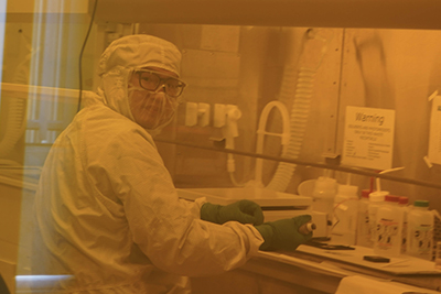
Josh Huang, technical program manager at Polaris Electro-Optics, fabricates a prototype device in the Qualcomm Institute’s Nano3 cleanroom. (Photo by Areli Alvarez)
“It’s very convenient for everything to happen in in the same environment, in the same ecosystem, so we can build things and move things very efficiently, quickly,” said Chiang of Polaris’s operations at QI. “That’s a huge plus.”
Pecinovsky added, “One measurement tool we use [at QI] is over a million dollars. There’s no way a startup company could buy one tool for a million dollars, let alone all the other infrastructure the institute provides. That has been invaluable.”
The QI location has also facilitated the on-boarding of interns from the UC San Diego student talent pool, providing cost-efficient staffing while offering an entrée into the working world for aspiring engineers.
“That’s also a huge win,” said Chiang, “that we can access talent here. The location is also very good. We have one colleague living in Carlsbad and another living in downtown, so it’s a perfect spot for both of them, and we have the trolley system available as well.”
Scaling Up
After several years of work on the device’s prototype, Polaris recently received a round of Series A funding, positioning the company to continue to develop its product all the way to launch.
According to Pecinovsky, a key challenge now is making the transition to producing the device at scale. “Right now we’re just doing onesies and twosies,” he said. “But for manufacturing, we need to be doing this by the million, on wafers, not on individual devices.”
Polaris’s VP of Engineering, Gianlorenzo Masini, who joined the company a year and a half ago from Cisco, noted: “The volumes needed are very high. And it’s only going to get larger. Data centers are so big that they need many, many of these [components].”
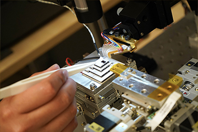
A prototype is manipulated in a configuration designed by Polaris Senior Photonics Engineer Jerome Jahn. (Photo by Areli Alvarez)
Masini noted not only are data centers growing, the use of optics is growing as well. “Basically, for the short links people still use copper cable, because it’s cheaper,” he said. “But as you increase the speed, the distance at which you can still use copper instead of optics gets smaller and smaller. More of these shorter links are being replaced with optics.”
As part of the process of scaling up production, the team is purchasing a new machine, an optical wafer prober, that will be installed in QI’s Atkinson Hall next to the Nano3 cleanroom. The optical wafer prober will evaluate devices that have been assembled by an outside contractor that could eventually mass produce them.
“[The optical wafer prober] is one of these tools that has to be on a concrete floor, on the first level of a building, with no vibration,” Pecinovsky said. “Again, that kind of thing that could really stymie a startup, but we are lucky that QI can accommodate us.”
In Dialogue
In the meantime, the Polaris team is building momentum by sending prototype devices to contacts in industry.
“We send it to them to evaluate,” said Pecinovsky. “We let them see for themselves that, ‘Yep, this is worth trying to push into production.’ Also, we need to make sure we’re on the right track and we’re meeting specifications they care about.”
“This morning, we were shipping samples to some of the big hyper-scalers,” Masini added. “That’s exciting.”
Pecinovsky is grateful to his team and to his financial and industrial partners for propelling the company this far.
“It’s a big challenge to produce totally new materials,” he said. “There’s no paper. We can’t pull up a reference for the recipe of how to do it. Everything has to be built. Having people who can figure it out is a critical part.”
Despite the challenges and the long hours, Pecinovsky has no regrets about his choice to leap into the unknown and found Polaris.
“I never aspired to be an entrepreneur,” he said. “But I’ve always liked doing hard things—from crossing the Alps on skis, to climbing 19,000 ft mountains in Peru and mountain biking across Guatemala. Starting Polaris is among the hardest things I’ve done, but like many hard things, that is part of what makes the experience meaningful. There is something uniquely sublime about the experience of creating technology that matters with an exceptional team of builders and weathering the ups and downs together.”
To learn more about Polaris Electro-Optics, see https://polariseo.com. To learn more about the Qualcomm Institute at UC San Diego, including the QI Innovation Space, Nano3 cleanroom and a Chip-Scale Photonics Testing facility, see http://qi.ucsd.edu.
Learn more about research and education at UC San Diego in: Artificial Intelligence


Stay in the Know
Keep up with all the latest from UC San Diego. Subscribe to the newsletter today.