Electrons Ripple Across Atom-Thin Layers of Carbon
By:
Published Date
Article Content

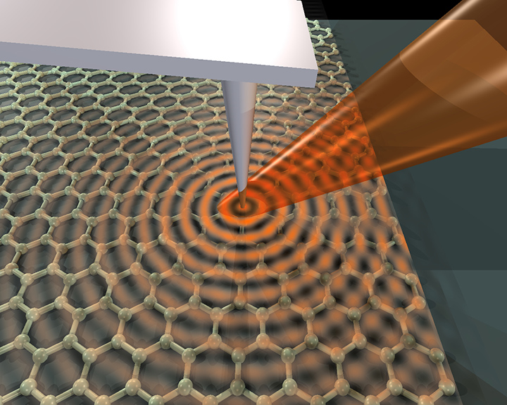
An infrared laser beam focused on the arm of an atomic-force microscope launches plasmons, waves through electrons, on the surface of graphene, a single honeycomb layer of linked carbon atoms. Credit: Basov Lab.
With a beam of infrared light, scientists have sent ripples of electrons along the surface of graphene and demonstrated that they can control the length and height of these oscillations, called plasmons, using a simple electrical circuit.
This is the first time anyone has observed plasmons on graphene, sheets of carbon just one atom thick with a host of intriguing physical properties, and an important step toward using plasmons to process and transmit information in spaces too tight to use light.
“Everybody suspected that plasmons should be there, but seeing is believing. We’ve imaged them and shown that they propagate. And we’ve demonstrated that we can control them,” said Dimitri Basov, professor of physics at the University of California, San Diego, and senior author of the report published online June 21 in advance of print publication in Nature.
To make the devices, they peeled graphene from graphite, the stuff of pencil lead, and rubbed it onto silicon dioxide chips.
They launched plasmons by shining an infrared laser on the surface of the graphene and measured the waves using the ultrasensitive arm of an atomic force microscope.
The outgoing waves are impossible to measure. But as they reach the edge of the graphene, they reflect like water waves from the wake of a boat bouncing off a pier.
Oscillations returning from the edge add to, or cancel out, subsequent waves, creating a characteristic interference pattern that reveals their wavelength and amplitude.
The scientists showed that pattern could be altered by controlling an electrical circuit formed with electrodes attached to the graphene surface and a layer of pure silicon beneath the chips.
“Here it is,” Basov said. “You just take a battery from a flashlight and crank the voltage and you have a tunable plasmonic device.”
Just like light can carry complex signals through fiber optics, plasmons could be used to transmit information. But plasmons could carry information within far tighter spaces.
“It’s impossible to confine light at nanometer scales because light wavelengths are many hundreds of nanometers,” said Zhe Fei, a graduate student in Basov’s lab and the first author of the paper. “We used light to excite surface plasmons with a length scale of 100 nanometers or less that can travel at very high speed from one side of the chip to the other.”
The performance they observed is promising. These are some of the shortest plasmon wavelengths measured in any material, yet the waves propagate as far as they do in metals like gold. And unlike plasmons on metals, graphene plasmons can be tuned.
A team of scientists working independently in Spain lead by Frank Koppens, Rainer Hillenbrand and Javier Garcia de Abajo has made a similar discovery using graphene film deposited by a gas rather than peeled from graphite. Their report, published in the same issue of Nature, bolsters this evidence for graphene plasmons.
“Graphene optoelectronics and information processing are very promising. We like to see our work contribute to future technology,” Basov said. “There also is entirely new, fundamental science coming out of this. By monitoring plasmons, we learn what electrons do in this new form of carbon, how fundamental interactions govern their properties. This is a path of inquiry.”
The Air Force Office of Scientific Research, Office of Naval Research, NASA, DARPA, University of California Office of the President and the National Science Foundation supported this work.
Additional authors on the paper include: A.S. Rodin, G.O. Andreev, A.S. McLeod, M. Wagner, M. Thiemens and M.M. Fogler, of UC San Diego; W. Bao, Zeng Zhao and C. N. Lau of UC Riverside; L. M. Zhang of Boston University; G. Dominguez of California State University, San Marcos; A. H. Castro-Neto of the National Research University of Singapore; and F. Keilmann of the Max Planck Institute of Quantum Optics and Center for Nanoscience in Garching, Germany.
Share This:
Stay in the Know
Keep up with all the latest from UC San Diego. Subscribe to the newsletter today.


