Improving Signal Amplification in Semiconductors and Other Optoelectronic Devices
Published Date
Article Content

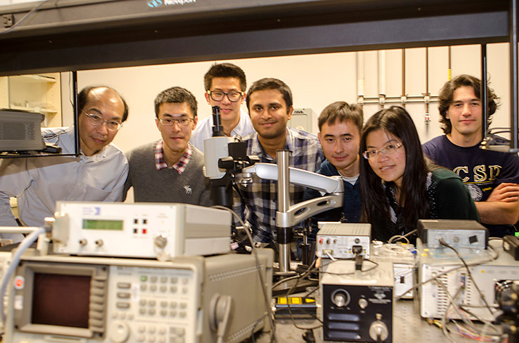
Electrical and Computer Engineering professor Yuhwa Lo and members of his team that demonstrated a new process for signal amplification in optoelectronic devices. Pictured (l-r): Yuhwa Lo, Yuchun Zhou, Alex Zhang, Iftikhar Niaz, Lujiang Yan, Yu-hsin Liu, Mahmut Kavrik. Co-authors not pictured: Physics Prof. Lu Sham and graduate student David Hall. [Photo by Victor Chen/Qualcomm Institute]
According to the American Institute of Physics (AIP), a new signal amplification process developed by researchers at the University of California, San Diego is “now poised to fuel new generations of electrical and photonic devices – transforming communications, imaging, and computing.”
The researchers in UC San Diego’s Jacobs School of Engineering, led by electrical and computer engineering professor Yuhwa Lo, have discovered a mechanism to amplify signals in optoelectronic systems that is far more efficient than the process long used by the semiconductor industry based on impact ionization.

ECE Prof. Yuhwa Lo is also chair of the Qualcomm Institute’s Nano3 faculty advisory committee. [Photo by Victor Chen/Qualcomm Institute]
"For many years, the semiconductor industry has relied on photodetectors for optoelectrical conversion, followed by low-noise electronic amplifiers to convert optical signals into electronic signals with amplification to enable information detection and processing," said Lo, who also oversees the Qualcomm Institute’s Nano3 nanofabrication facility, where the new technique was tested. “Avalanche photodetectors that use impact ionization became the devices of choice and have remained so for many decades,” in spite of their high operating voltage – typically 30 to 200 volts – and rapidly worsening noise with amplification.
Writing in AIP Publishing’s Applied Physics Letters, Lo and his collaborators, including physics professor emeritus Lu Sham, report on a far more efficient mechanism to amplify signals. They dubbed it the ‘cycling excitation process,’ or CEP.
Hoping to reduce voltage (power) and noise, the UC San Diego team looked at the complex interactions among electrons in localized and extended states and phonons (a unit of vibrational energy arising from oscillating atoms within a crystal).
Like with most semiconductors, the device demonstrated at UC San Diego has a p/n junction, a boundary between two semiconductor materials within a single crystal of semiconductor. The structure is called a ‘heavily compensated p/n junction’ because, said Lo, “the only unique feature is that both sides of the p/n junction contain a substantial amount of counter doping,” i.e., a large number of donors exist in the p-region, with acceptors in the n-region.

This schematic illustrates the concepts involved in the cycling excitation process. [Photo courtesy Yuchun Zhou/UC San Diego]
According to the Jan. 20 AIP news release, “counter impurities in the compensated p/n junction are responsible for the team's highly efficient signal (photocurrent) amplification process.” Electrons or holes crossing the depletion region gain kinetic energy and, in turn, excite new electron-hole pairs using the compensating impurities (donors in the p-side and acceptors on the n-side) as intermediate states.
"An energetic electron, for example, can excite an electron from an occupied acceptor to the conduction band, while a phonon is absorbed subsequently to fill the acceptor with an electron from the valence band - producing a hole in the valence band to complete the generation of an electron-hole pair," said Yuchun Zhou, first author of the paper in Applied Physics Letters and a Ph.D. student in Lo's group. "This type of process occurs on both sides of the p/n junction and forms cycles of electron-hole excitation to produce high gain."
The key discovery and innovation for the amplification process was the use of compensating impurities as the intermediate steps for electron-hole pair generation. Explained Lo: "Impurity states are localized, so the conservation of momentum that limits the efficiency for conventional impact ionization can be greatly relaxed and leads to higher signal amplification efficiency and reduced operation voltage."
The UC San Diego researcher also observed that perhaps an entirely new physical mechanism can be found “in the most common device structure – a p/n junction – that has been used since the semiconductor industry’s heyday. It appears that a small modification, such as heavy doping compensation, from a common structure can be used to take advantage of the unusual physical process that results from concerted interactions between electrons in extended and localized (impurity) states and phonons.”
The team believes that the new signal amplification mechanism could be used in a wide array of devices and semiconductors, creating a new paradigm for the semiconductor industry.
"With an efficient gain mechanism at an operation voltage compatible with CMOS integrated circuits, it's possible to produce communication and imaging devices with superior sensitivity at a low cost," Lo pointed out. "By using other methods along with optical excitation to produce the seed carriers that initiate the cycling excitation process, we can conceive new types of transistors and circuits and extend the scope of applications beyond optical detection."
Share This:
You May Also Like
Stay in the Know
Keep up with all the latest from UC San Diego. Subscribe to the newsletter today.


